The cracking directly affects the performance of photovoltaic modules, and it is also one of the defects that need to be tested and sorted in the production of battery chips. With the development of photoelectric technology and machine vision image detection technology, EL has become the main means to detect defects such as solar cracking. The focus of the editor is to sort out the causes of the cracks in the battery and the current mainstream detection and identification methods. The cracking directly affects the performance of photovoltaic modules, and it is also one of the defects that need to be tested and sorted in the production of battery chips. With the development of photoelectric technology and machine vision image detection technology, EL has become the main means to detect defects such as solar cracking. The focus of the editor is to sort out the causes of the cracks in the battery and the current mainstream detection and identification methods. 1. What is “hidden crack� The crack is a common defect in the battery. Due to the nature of the crystal structure, crystalline silicon cells are very susceptible to cracking. The process flow of crystalline silicon module production is long, and many parts may cause the cell to crack. The essential cause of cracking can be summarized as mechanical stress or thermal stress on the silicon wafer. In recent years, in order to reduce the cost, crystalline silicon cell manufacturers have been developing in a thinner and thinner direction, thereby reducing the ability of the cell to prevent mechanical damage. In 2011, Germany's ISFH published their findings: according to the shape of the cell crack, it can be divided into five categories: tree cracks, synthetic cracks, oblique cracks, parallel to the main grid lines, perpendicular to the grid lines and throughout the entire Crack in the battery.
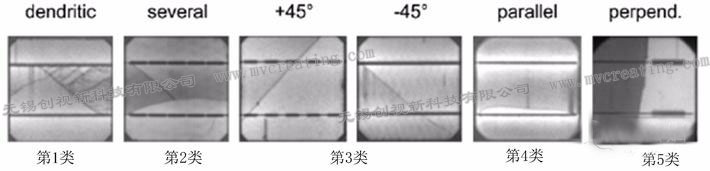 Figure 1: Crystalline silicon cell crack shape 2, "clear crack" on the performance of the module Different crack shape, position, the impact on the function of the battery is not the same, let us first look at the amplification of a battery Take a look at the picture.
 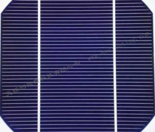 Figure 2: Crystal silicon cell structure According to the structure of the crystalline silicon cell, as shown in the above figure, the current generated by the cell depends on the "main gate line of the surface and the fine gate line perpendicular to the main gate line" to collect and derive. When the crack causes the fine gate line to break, the fine gate line cannot transport the collected current to the main gate line, which will cause partial or even partial failure of the cell. For the above reasons, the most influential effect on the function of the cell is the crack (parallel 4) parallel to the main gate line. According to the results of the study, 50% of the failed sheets are from cracks parallel to the main grid lines. The efficiency loss of a 45° oblique crack (Category 3) is 1/4 of the loss parallel to the main grid line. Cracks perpendicular to the main gate line (Category 5) hardly affect the fine grid lines, thus causing the area of ​​the cell failure to be almost zero. Compared with the gate line of the surface of the crystalline silicon cell, the surface of the thin film battery is entirely covered with a transparent conductive film, so this is also a reason why the thin film component has no crack. Studies have shown that when the failure area of ​​a single cell in a component is less than 8%, the power of the component is not affected much, and 2/3 of the diagonal stripes in the component have no effect on the power stability of the component. Therefore, when the cell in the module is cracked, there may be a loss of efficiency, but it is not necessary to talk about the "discoloration" of the crack. 3. The main method for detecting "cracking" defects EL (Electroluminescence) is a simple and effective method for detecting cracks. The detection principle is as follows. The core part of the cell is a semiconductor PN junction. Under other conditions (such as illumination, voltage, temperature), the inside is in a dynamic equilibrium state, and the number of electrons and holes is relatively stable. If a voltage is applied, the internal electric field in the semiconductor will be weakened, and the electrons in the N region will be pushed toward the P region, recombining with the holes in the P region (it is also understood that the holes in the P region are pushed toward the N region, and N The electron recombination of the region, after the recombination, is additionally emitted in the form of light, that is, electroluminescence. When a forward bias is applied, the crystalline silicon cell emits light at a wavelength of about 1100 nm, which belongs to the infrared band and is not visible to the naked eye. Therefore, when performing the EL test, it is necessary to use a CCD camera to assist in capturing these photons, and then display them in the form of an image by computer processing. After applying a voltage to the crystalline silicon component, the more the number of electrons and holes recombine is, the more photons are emitted, and the brighter the measured EL image is. If there is a region EL image comparison Dark, indicating that there are fewer electrons and holes generated in the area (such as the middle of the battery in Figure 3), indicating that there is a defect (composite center); if some areas are completely dark, it means that there is no electron and space The composite of the holes (marked by the red line in Figures 3 and 4), or the illuminance is blocked by other obstacles (at the main grid lines in Figures 3 and 4), the signal cannot be detected.
 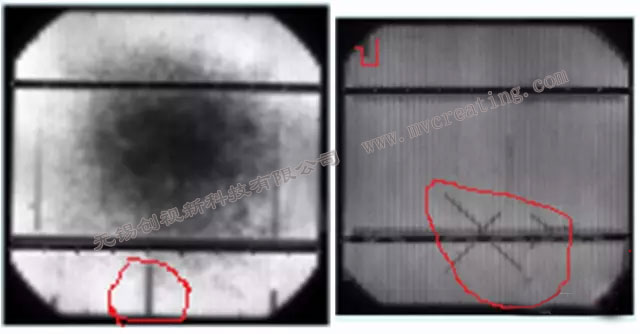 Figure 3 Black-hearted piece Figure 4: The crack in the middle of the figure is because the size of the component is too large, and the image is stitched, which is normal.
 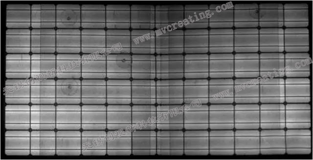 Figure 5 Normal component EL image 4, summary 1) There are many kinds of cracks, not all cracks will affect the performance of the battery; 2) In the production, transportation, installation and maintenance of components, taking into account the crystalline silicon components The cracking feature also needs to improve and refine the operation process in each process segment and handling and construction process to reduce the possibility of component cracking. At the same time, it strengthens the crack detection of the silicon wafer in the raw material link to avoid the occurrence of crack defects. Raw materials flow into the next process. 3) EL is the simplest and most effective way to detect cracks. Http://news.chinawj.com.cn
  Editor: (Hardware Business Network Information Center) http://news.chinawj.com.cn
Oil Water Separator,Oil And Water Separator,Water Oil Separator System,Industrial Oil Water Separator
FRANCOOL TECHNOLOGY (SHENZHEN)CO., LTD , https://www.francoolcn.com