Phase measurement has been widely used in many fields such as industrial automation instrumentation, intelligent control and communication electronics. The requirements for phase measurement are gradually developing towards high precision and intelligence. For low-frequency phase measurement, the digital pulse filling method is generally used to measure the phase of the input signal. However, in order to meet certain measurement accuracy, the clock frequency of the microprocessor is required to be sufficiently high.
Similarly, when using this method to measure high-frequency signals, because the phase difference is relatively small, the general microprocessor clock frequency can not meet the high-precision counting requirements, which will inevitably affect the accuracy of phase measurement. Therefore, the counting frequency of the standard clock must be increased to meet the measurement requirements. In this way, on the one hand, the difficulty of the design itself is increased, and on the other hand, the requirements for selecting components are also improved. The system first uses the frequency conversion method to convert the high-frequency input signal into a low-frequency signal, and keeps the phase of the original signal unchanged, and then uses the digital phase measuring system based on the ADuC7128 as the control core to perform measurement, thereby completing the broadband input signal. Phase measurement.
1 Introduction of the principle of difference frequency conversion
The measured signal and reference signal are described in the following form using a mathematical model:
Measured signal: 
Reference signal: 
Where: A is the amplitude of the signal under test; B is the amplitude of the reference signal; f is the frequency of the signal under test; f0 is the frequency of the reference signal; θ is the amplitude of the signal under test.
At the same time, the two signals y1 and y2 are sent to the mixer for multiplication by the mixing operation, and the signal y3 is obtained.
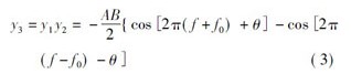
Then y3 is sent to the low-pass filter for filtering, and the high-frequency signal is filtered out. The remaining low-frequency signal mathematical expression is:
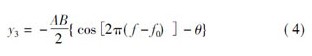
Compared with y1, y3 has a linear change in amplitude, but the amplitude does not change, but the frequency decreases. The frequency is the frequency difference between the measured signal and the reference signal. For measuring y3, it is much easier than measuring y1 directly. By applying the difference frequency transform method to the phase measurement of the high frequency signal, the accuracy of the phase measurement can be improved, and the frequency band of the input signal can be widened.
2 Digital phase measurement system design
2.1 Hardware structure design As shown in Figure 1, the system is mainly composed of signal conditioning circuit, frequency conversion circuit and microprocessor control circuit.

2.1.1 Signal Conditioning Circuit The signal conditioning circuit must complete the functions of coupling, attenuation, amplification, level adjustment, etc. of the input signal. The front-end analog channel with good performance is necessary for high-precision measurement [3]. The two signal conditioning channels CH1 and CH2 in this design have exactly the same symmetrical structure, and at the same time signal conditioning the input signal.
2.1.2 Frequency Conversion Circuit The analog multiplier is an electronic device that performs the multiplication of two analog signals, since the multiplier has better linearity than the double balanced mixer. Therefore, this design uses ADAD chip of Analog Devices as the mixer of the system. The AD834 is used to mix the signal to be tested with the reference signal generated by the internal DDS module of ADuC7128, and then the difference frequency signal is single-ended voltage signal. Mode output.
The frequency conversion circuit is shown in Figure 2. The pins X1 and Y2 of the AD834 are connected to the ground, and the signal to be tested and the reference signal are input to the two signal ports Y1 and X2 of the AD834 in a single-ended input. Select Y1 and X2 as single-ended input pins because these two pins are far from the output. Selecting them as inputs can reduce the coupling component of the input signal to the output. According to the design requirements, an op amp OP-07 with high open-loop gain is connected behind the AD834, and an I/V conversion circuit is formed by OP-7 and R7 and R6, so that the output signal of the multiplier can be formed by the double-ended differential current. Converted to a single-ended voltage form.
Hot-Melt Bookbinding Adhesives
The term [perfect binding" was created in 1911 to describe the hot-melt adhesive application in the bookbinding process.
At that time, hot melts attempted to overcome the disadvantages of emulsion adhesives while retaining the desirable characteristics of pull strength and flexibility. The driving force toward hot-melt adhesives was their high speed, minimal waste, and relatively low cost.
Our company chaobang adhesive co., Ltd. set up in 1999, we are professional Hot Melt Glue manufacture. Our company has been committed to the Bookbinding Glue for nearly 20 years. In the company's development process, we meet with many different questions and we solved those questions. our company has been developing steadily. We are trying to get better and better. We must do our best to make the good quality product, we must produce the suitable product for the market. Believe us, chose us is right.


Bookbinding Glue
Book Binding Glue,Book Binding Adhesive,Paper Binding Glue,Book Binding Tape
Taixing Chaobang Adhesive Co., Ltd. , http://www.cb-adhesive.com